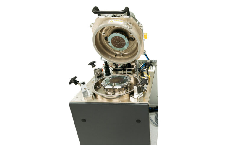
EVG 501-Hot Embossing
The EVG501 is a highly flexible wafer bonding system that can handle substrate sizes from single chips to 150 mm (200 mm in case of a 200 mm bond chamber).
Product Desription
The EVG501 is a highly flexible wafer bonding system that can handle substrate sizes from single chips to 150 mm (200 mm in case of a 200 mm bond chamber). This tool supports all common wafer bonding processes such as anodic, glass frit, solder, eutectic, transient liquid phase, and direct. The easy access bond chamber and tooling design allows for quick and easy retooling for different wafer sizes and processes with a conversion time of less than 5 minutes. This versatility is ideal for universities, R&D facilities, or low-volume production. The design of the bond chambers is the same on the EVG high-volume-manufacturing tools, such as the EVG GEMINI, and the bonding recipes are easily transferable, allowing for easy scale up of production volumes.
Product Highlights
Application
Variable substrate
For up to 150 mm wafers
Maximum contact force
20 kN
Vacuum
Standard: 0.1 mbar; optional: 1E-5 mbar


