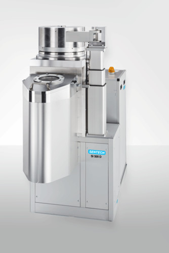


DUE TO LOW İON ENERGY AND NARROW İON ENERGY DİSTRİBUTİON, LOW DAMAGE ETCHİNG AND NANO STRUCTURİNG CAN BE PERFORMED WİTH OUR İCP PLASMA ETCHİNG TOOLS.
The SI 500 ICP plasma etching tool is configured for processing III-V compound semiconductors (GaAs, InP, GaN, InSb). This equipement is used to etch nanometric size patterns with high aspect ratio(photonic crystals, nanopilars,..) and micrometric patterns up to 20µm high.
Due to low ion energy and narrow ion energy distribution, low damage etching andnano structuring can be performed with our icp plasma etching tools.
High rate plasma etching of Si for MEMS with high aspect ratio is easily performed either using room temperature alternating processes or cryogenicprocesses for smooth side walls.
The Planar Triple Spiral Antenna (PTSA) source is a unique feature of SENTECH high end plasma process systems. The PTSA source generates homogeneous plasma with high ion density and low ion energy. It features high coupling efficiency and very good ignition behavior for processing of a large variety of materials and structures.