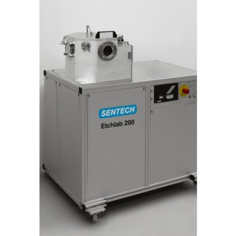


The Etchlab 200 plasma etcher can be configured for processing of materials that are compatible with wafer direct loading, including but not limited to silicon and silicon compounds, compound semiconductors, dielectrics, and metals.
The Etchlab 200 RIE plasma etcher represents a family of direct load plasma etcher combining the advantages of a parallel plate electrode design for RIE with the cost effective design of direct load. The Etchlab 200 features simple and fast sample loading from parts to 200 mm or 300 mm diameter wafer directly onto the electrode or on carrier. Flexibility, modularity, and a small footprint are design characteristics of the Etchlab 200. Large diagnostic windows located at the top electrode and the reactor can easily accommodate the SENTECH laser interferometer or OES and RGA systems. Ellipsometer ports are available for process monitoring using SENTECH insitu ellipsometers.
The Etchlab 200 plasma etcher can be configured for processing of materials that are compatible with wafer direct loading, including but not limited to silicon and silicon compounds, compound semiconductors, dielectrics, and metals.
RIE plasma etcher Etchlab 200 combines parallel plate plasma source design with direct load.
According to its modular design, the plasma etcher Etchlab 200 is upgradeable with larger pumping unit, vacuum load lock, and additional gas lines.
This plasma etcher is equipped with a user-friendly powerful software with mimic GUI, parameter window, recipe editor, data logging, user management.